RankRizz

Semiconductor Electronics — JEE Main Previous Year Questions

Every Semiconductor Electronics question JEE Main has set from 2004–2026, grouped by the idea it tests rather than the order of the syllabus. 253 questions across 6 distinct ideas. Free to read, answer key on every one.

Questions

253

Distinct ideas

6

Share of marks

4.4%

Difficulty

EASY

The ideas inside Semiconductor Electronics

A chapter is not one subject — it is a handful of procedures the examiner reuses. These are the ones Semiconductor Electronics questions actually test.

Every Semiconductor Electronics question

141–160 OF 253 · NEWEST FIRST

JEE MAIN 2021 · 20 JUL S1p-n junction diode and its characteristicsTRANSCRIBED

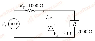
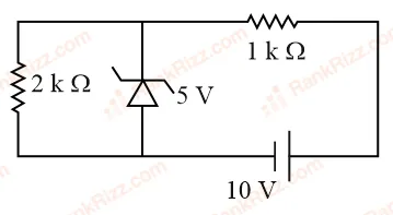
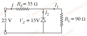
For the circuit shown below, calculate the value of IzI_z:

Figure for JEE Main 2021 Physics question on p-n junction diode and its characteristics
  1. A

    25 mA

  2. B

    0.15 A

  3. C

    0.1 A

  4. D

    0.05 A

JEE MAIN 2021 · 31 AUG S1Logic gates and digital circuitsTRANSCRIBED

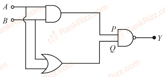
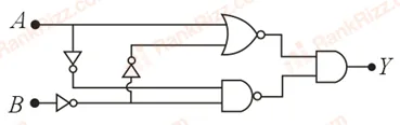
In the following logic circuit the sequence of the inputs AA, BB are (0,0),(0,1),(1,0)(0, 0), (0, 1), (1, 0) and (1,1)(1, 1). The output YY for this sequence will be:

Figure for JEE Main 2021 Physics question on Logic gates and digital circuits
  1. A

    0, 1, 0, 1

  2. B

    0, 0, 1, 1

  3. C

    1, 1, 1, 0

  4. D

    1, 0, 1, 0

JEE MAIN 2021 · 27 JUL S2Logic gates and digital circuitsTRANSCRIBED

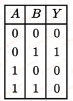
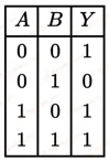
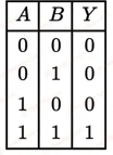
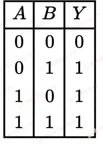
Find the truth table for the function Y of A and B represented in the following figure.
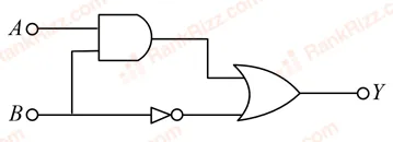
Figure for JEE Main 2021 Physics question on Logic gates and digital circuits
  1. A
    Figure for JEE Main 2021 Physics question on Logic gates and digital circuits
  2. B
    Figure for JEE Main 2021 Physics question on Logic gates and digital circuits
  3. C
    Figure for JEE Main 2021 Physics question on Logic gates and digital circuits
  4. D
    Figure for JEE Main 2021 Physics question on Logic gates and digital circuits
JEE MAIN 2021 · 31 AUG S2p-n junction diode and its characteristicsTRANSCRIBED

Statement I: To get a steady DC output from the pulsating voltage received from a full wave rectifier we can connect a capacitor across the output parallel to the load RLR_L.
Statement II: To get a steady DC output from the pulsating voltage received from a full wave rectifier we can connect an inductor in series with RLR_L.
In the light of the above statements, choose the most appropriate answer from the options given below:

  1. A

    Both Statement I and Statement II are false

  2. B

    Both Statement I and Statement II are true

  3. C

    Statement I is false but Statement II is true

  4. D

    Statement I is true but Statement II is false

JEE MAIN 2021 · 01 SEP S2p-n junction diode and its characteristicsTRANSCRIBED

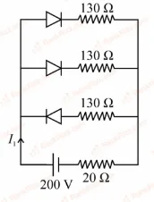
In the given figure, each diode has a forward bias resistance of 30 Ω\Omega and infinite resistance in reverse bias. The current I1I_1 will be:

Figure for JEE Main 2021 Physics question on p-n junction diode and its characteristics
  1. A

    2.0 A

  2. B

    3.75 A

  3. C

    2.73 A

  4. D

    2.35 A

JEE MAIN 2021 · 26 FEB S2Logic gates and digital circuitsTRANSCRIBED

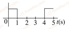
Draw the output signal Y in the given combination of gates.
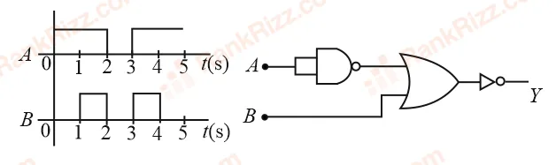
Figure for JEE Main 2021 Physics question on Logic gates and digital circuits
  1. A
    Figure for JEE Main 2021 Physics question on Logic gates and digital circuits
  2. B
    Figure for JEE Main 2021 Physics question on Logic gates and digital circuits
  3. C
    Figure for JEE Main 2021 Physics question on Logic gates and digital circuits
  4. D
    Figure for JEE Main 2021 Physics question on Logic gates and digital circuits
JEE MAIN 2021 · 25 JUL S2p-n junction diode and its characteristicsTRANSCRIBED

In a semiconductor, the number density of intrinsic charge carriers at 27°C is 1.5×10161.5 \times 10^{16} m−3^{-3}. If the semiconductor is doped with an impurity atom, the hole density increases to 4.5×10224.5 \times 10^{22} m−3^{-3}. The electron density in the doped semiconductor is _________ ×109\times 10^{9} m−3^{-3}

JEE MAIN 2021 · 24 FEB S1p-n junction diode and its characteristicsTRANSCRIBED

In connection with the circuit drawn below, the value of current flowing through 2 kΩ\Omega resistor is ______ ×10−4\times 10^{-4} A.

Figure for JEE Main 2021 Physics question on p-n junction diode and its characteristics
JEE MAIN 2021 · 16 MAR S1Zener diode, LED, photodiode and solar cellTRANSCRIBED

The value of power dissipated across the zener diode (Vz=15V_z = 15 V) connected in the circuit as shown in the figure is x×10−1x \times 10^{-1} W.

Figure for JEE Main 2021 Physics question on Zener diode, LED, photodiode and solar cell


The value of xx to the nearest integer is ________.

JEE MAIN 2021 · 18 MAR S2Transistors (older syllabus)TRANSCRIBED

The typical output characteristics curve for a transistor working in the common-emitter configuration is shown in the figure.
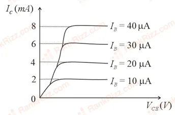
Figure for JEE Main 2021 Physics question on Transistors (older syllabus)


The estimated current gain from the figure is ___.

JEE MAIN 2021 · 27 AUG S1Transistors (older syllabus)TRANSCRIBED

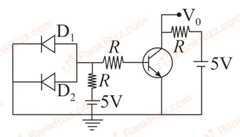
A circuit is arranged as shown in figure. The output voltage V0V_0 is equal to _________ V.

Figure for JEE Main 2021 Physics question on Transistors (older syllabus)
JEE MAIN 2021 · 27 JUL S1Transistors (older syllabus)TRANSCRIBED

A transistor is connected in common emitter circuit configuration, the collector supply voltage is 10 V and the voltage drop across a resistor of 1000 Ω\Omega in the collector circuit is 0.6 V. If the current gain factor (β)(\beta) is 24, then the base current is _________ μ\muA. (Round off to the Nearest Integer)

JEE MAIN 2021 · 20 JUL S2Zener diode, LED, photodiode and solar cellTRANSCRIBED

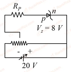
A zener diode having zener voltage 8 V and power dissipation rating of 0.5 W is connected across a potential divider arranged with maximum potential drop across zener diode as shown in the diagram. The value of protective resistance RpR_p is ___ Ω\Omega.

Figure for JEE Main 2021 Physics question on Zener diode, LED, photodiode and solar cell
JEE MAIN 2021 · 26 FEB S2Zener diode, LED, photodiode and solar cellTRANSCRIBED

The zener diode has a Vz=30V_z = 30 V. The current passing through the diode for the following circuit is ______ mA.
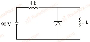
Figure for JEE Main 2021 Physics question on Zener diode, LED, photodiode and solar cell
JEE MAIN 2021 · 16 MAR S1Logic gates and digital circuitsTRANSCRIBED

In the logic circuit shown in the figure, if input AA and BB are 0 to 1 respectively, the output at YY would be xx. The value of xx is ________.

Figure for JEE Main 2021 Physics question on Logic gates and digital circuits
JEE MAIN 2021 · 27 AUG S2Zener diode, LED, photodiode and solar cellTRANSCRIBED

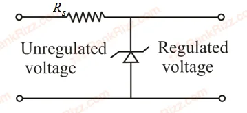
A zener diode of power rating 2 W is to be used as a voltage regulator. If the zener diode has a breakdown of 10 V and it has to regulate voltage fluctuated between 6 V and 14 V, the value of RsR_s for safe operation should be _________ Ω\Omega.

Figure for JEE Main 2021 Physics question on Zener diode, LED, photodiode and solar cell
JEE MAIN 2021 · 20 JUL S2p-n junction diode and its characteristicsTRANSCRIBED

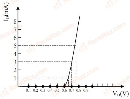
For the forward biased diode characteristics shown in the figure, the dynamic resistance at ID=3I_D = 3 mA will be ___ Ω\Omega.

Figure for JEE Main 2021 Physics question on p-n junction diode and its characteristics
JEE MAIN 2021 · 22 JUL S1Zener diode, LED, photodiode and solar cellTRANSCRIBED

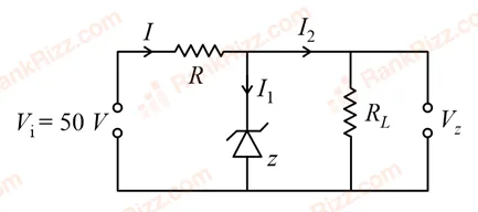
In a given circuit diagram, a 5 V zener diode along with a series resistance is connected across a 50 V power supply. The minimum value of the resistance required, if the maximum zener current is 90 mA will be ___ Ω\Omega.

Figure for JEE Main 2021 Physics question on Zener diode, LED, photodiode and solar cell
JEE MAIN 2021 · 26 AUG S2Zener diode, LED, photodiode and solar cellTRANSCRIBED

For the given circuit, the power across zener diode is _________ mW.
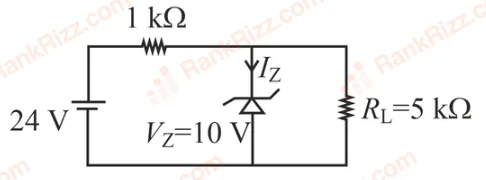
Figure for JEE Main 2021 Physics question on Zener diode, LED, photodiode and solar cell
JEE MAIN 2020 · 07 JAN S2Diode circuits and rectifiersTRANSCRIBED

In the figure, potential difference between A and B is:
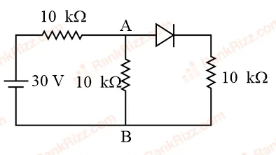
Figure for JEE Main 2020 Physics question on Diode circuits and rectifiers
  1. A

    10 V

  2. B

    5 V

  3. C

    15 V

  4. D

    0 V