JEE MAIN 2026 · 21 JAN S2p-n junction diode and its characteristicsTRANSCRIBED
The charge stored by the capacitor C in the given circuit in the steady state is ______ .
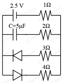
- A
7.5
- B
5
- C
10
- D
12.5
Every JEE Main question on p-n junction diode and its characteristics, one of the ideas inside Semiconductor Electronics: 55 questions from 2004–2026, 29 of them in the last five years. Newest first, answer key on every one. Free to read.
Questions
55
Years asked
15
Since
2004
Of the chapter
22%
Questions on p-n junction diode and its characteristics in each year it was asked, the latest 12 of 15.
1–20 OF 55 · NEWEST FIRST
The charge stored by the capacitor C in the given circuit in the steady state is ______ .
7.5
5
10
12.5
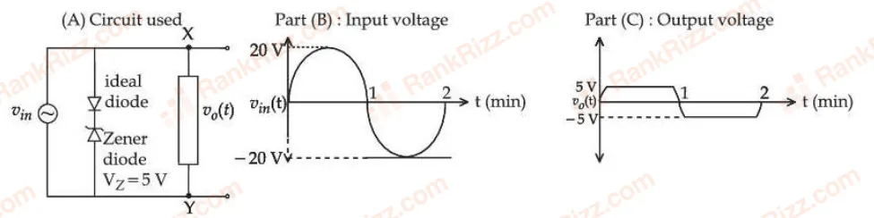
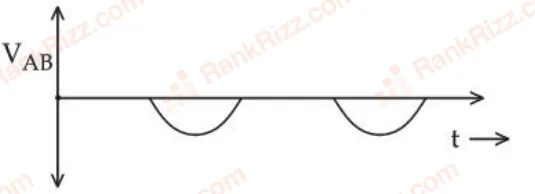
For the given circuit (shown in part (A)) the time dependent input voltage and corresponding output are shown in part (B) and part (C), respectively. Identify the components that are used in the circuit between points X and Y.




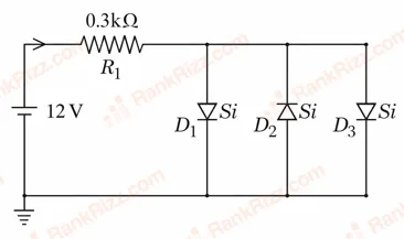
Assuming in forward bias condition there is a voltage drop of 0.7V across a silicon diode, the current through diode in the circuit is ___ mA.
(Assume all diodes in the given circuit are identical)
18.8
17.6
11.7
20.15
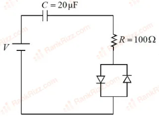
Consider a circuit consisting of a capacitor (20 F), resistor (100 ) and two identical diodes as shown in figure. The resistance of diode under forward biasing condition is 10 . The time constant of the circuit is s. The value of is :
Given below are two statements: one is labelled as Assertion A and the other is labelled as Reason R
Assertion A: A diode under reverse-biased condition provides very small current which is nearly independent of voltage until a critical limit at which the current increases drastically.
Reason R: Below the critical voltage limit, only majority charge carriers flow which increases drastically above critical voltage.
Choose the correct answer from the options given below :
Both A and R are true, and R is the correct explanation of A
Both A and R are true, but R is NOT the correct explanation of A
A is true but R is false
A is false but R is true
In a semiconductor p-n diode, the doping concentrations on p-side has atoms/cm³ and the n-side has atoms/cm³respectively. Which one of the following statements is true?
Widths of depletion region on either side of the interface are equal
The depletion region widths is more on p-side compared to that in n-side
The depletion region width is more on n-side compared to that the p-side
No depletion region forms because of unequal doping concentrations on p and n-sides
Which of the following circuits represents a forward biased diode?
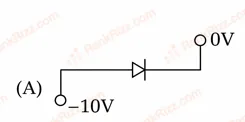
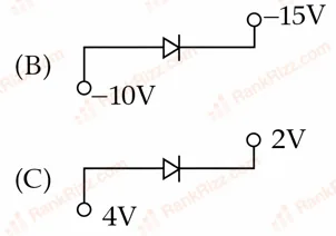
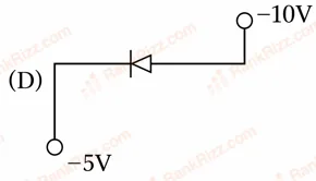
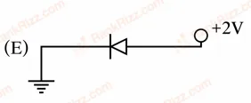
Choose the correct answer from the options given below :
(A) and (D) only
(B), (D) and (E) only
(C) and (E) only
(B), (C) and (E) only
The output voltage in the following circuit is (Consider ideal diode case) :
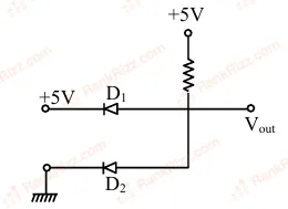
10 V
0 V
+5 V
-5 V
Consider a n-type semiconductor in which and are number of electrons and holes, respectively.
(A) Holes are minority carriers
(B) The dopant is a pentavalent atom
(C)
(where is number of electrons or holes in semiconductor when it is intrinsic form)
(D)
(E) The holes are not generated due to the donors
Choose the correct answer from the options given below :
(A), (C), (D) only
(A), (C), (E) only
(A), (B), (E) only
(A), (B), (C) only
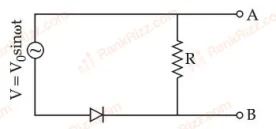
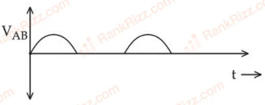
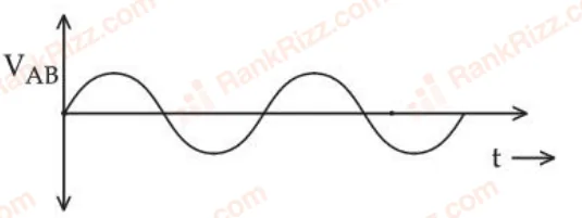
In the circuit shown here, assuming threshold voltage of diode is negligibly small, then voltage is correctly represented by :
would be zero at all times
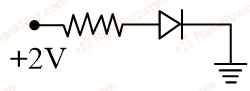
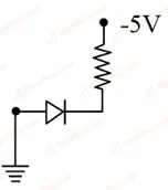
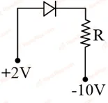
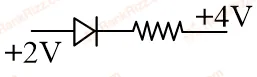
Which of the following circuits is reverse-biased?
In the given circuit, the voltage across load resistance is:
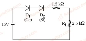
8.75 V
9.00 V
8.50 V
14.00 V
The acceptor level of a p-type semiconductor is . The maximum wavelength of light which can create a hole would be : Given .
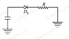
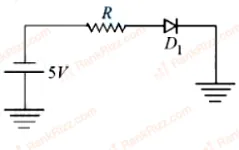
Which of the diode circuit shows correct biasing used for the measurement of dynamic resistance of p-n junction diode:
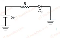
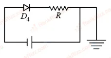
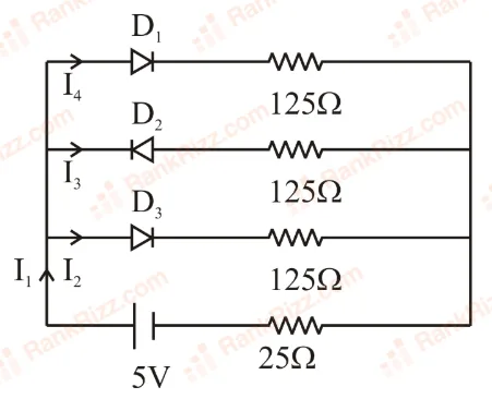
If each diode has a forward bias resistance of 25 in the below circuit, which of the following options is correct?
The effect of increase in temperature on the number of electrons in conduction band and resistance of a semiconductor will be as:
Both and resistance decrease
Both and resistance increase
increases, resistance decreases
decreases, resistance increases
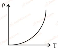
The resistivity of semiconductor varies with temperature. Which of the following curve represents the correct behaviour?
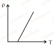
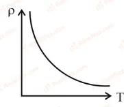
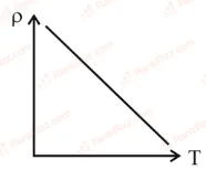
Given below are two statements: one is labelled as Assertion A and the other is labelled as Reason R
Assertion A: Diffusion current in a p-n junction is greater than the drift current in magnitude if the junction is forward biased.
Reason R: Diffusion current in a p-n junction is from the n-side to the p-side if the junction is forward biased.
Both A and R are correct but R is NOT the correct explanation of A
A is correct but R is not correct
A is not correct but R is correct
Both A and R is correct and R is the correct explanation of A
Match the List I with List II
A. Intrinsic Semiconductor I. Fermi-level near valence band
B. n-type semiconductor II. Fermi-level at middle of valence and conduction band
C. p-type semiconductor III. Fermi-level near conduction band
D. Metals IV. Fermi-level inside conduction band
(A) I, (B) II, (C) III, (D) IV
(A) II, (B) I, (C) III, (D) IV
(A) II, (B) III, (C) I, (D) IV
(A) III, (B) I, (C) II, (D) IV
Statement I: When a Si sample is doped with Boron, it becomes P type and when doped by Arsenic it becomes N-type semi conductor such that P-type has excess holes and N-type has excess electrons.
Statement II: When such P-type and N-type semi-conductors, are fused to make a junction, a current will automatically flow which can be detected with an externally connected ammeter.
In the light of above statements, choose the most appropriate answer from the options given below.
Both Statement I and statement II are incorrect
Statement I is incorrect but statement II is correct
Both Statement I and statement II are correct
Statement I is correct but statement II is incorrect