RankRizz

Transistors (older syllabus) — JEE Main Previous Year Questions

Every JEE Main question on Transistors (older syllabus), one of the ideas inside Semiconductor Electronics: 42 questions from 2004–2023, 28 of them in the last five years. Newest first, answer key on every one. Free to read.

Questions

42

Years asked

13

Since

2004

Of the chapter

17%

Every Transistors (older syllabus) question

21–40 OF 42 · NEWEST FIRST

JEE MAIN 2021 · 27 JUL S1Transistors (older syllabus)TRANSCRIBED

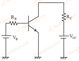
A transistor is connected in common emitter circuit configuration, the collector supply voltage is 10 V and the voltage drop across a resistor of 1000 Ω\Omega in the collector circuit is 0.6 V. If the current gain factor (β)(\beta) is 24, then the base current is _________ μ\muA. (Round off to the Nearest Integer)
JEE MAIN 2020 · 06 SEP S2Transistors (older syllabus)TRANSCRIBED

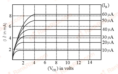
The output characteristics of a transistor is shown in the figure. When VCEV_{CE} is 10 V10\,\text{V} and IC=4.0 mAI_C = 4.0\,\text{mA}, then value of βac\beta_{ac} is___

Figure for JEE Main 2020 Physics question on Transistors (older syllabus)
JEE MAIN 2019 · 10 APR S1Transistors (older syllabus)TRANSCRIBED

An NPN transistor operates as a common emitter amplifier, with a power gain of 60 dB. The input circuit resistance is 100 Ω and the output load resistance is 10 kΩ. The common emitter current gain β is:

  1. A

    6×1026 \times 10^2

  2. B

    10210^2

  3. C

    10410^4

  4. D

    60

JEE MAIN 2019 · 12 JAN S2Transistors (older syllabus)TRANSCRIBED

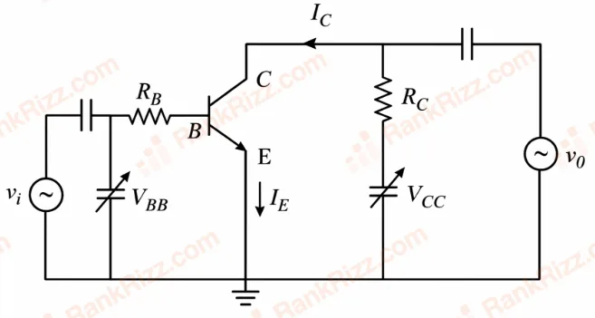
In the figure, given that VBBV_{BB} supply can vary from 0 to 5.0 V, VCC=5V_{CC} = 5 V, βdc=200\beta_{dc} = 200, RB=100R_B = 100 kΩ\Omega, RC=1R_C = 1 kΩ\Omega and VBE=1.0V_{BE} = 1.0 V. The minimum base current and the input voltage at which the transistor will go to saturation, will be, respectively:

Figure for JEE Main 2019 Physics question on Transistors (older syllabus)
  1. A

    25μA25 \mu A and 2.8 V

  2. B

    20μA20\mu A and 2.8V

  3. C

    25μA25\mu A and 3.5V

  4. D

    20μA20\mu A and 3.5V

JEE MAIN 2019 · 08 APR S2Transistors (older syllabus)TRANSCRIBED

A common emitter amplifier circuit, built using an NPN transistor, is shown in the figure. Its dc current gain is 250, RC=1R_C = 1 kΩ\Omega and VCC=10V_{CC} = 10 V. The minimum base current for VCEV_{CE} to reach saturation is:

Figure for JEE Main 2019 Physics question on Transistors (older syllabus)
  1. A

    10 μ\muA

  2. B

    40 μ\muA

  3. C

    7 μ\muA

  4. D

    100 μ\muA

JEE MAIN 2019 · 09 APR S1Transistors (older syllabus)TRANSCRIBED

An NPN transistor is used in common emitter configuration as an amplifier with 1 kΩ\Omega load resistance. Signal voltage of 10 mV is applied across the base-emitter. This produces a 3 mA change in the collector current and 15 μ\muA change in the base current of the amplifier. The input resistance and voltage gain are:

  1. A

    0.33 kΩ\Omega, 1.5

  2. B

    0.67 kΩ\Omega, 300

  3. C

    0.67 kΩ\Omega, 200

  4. D

    0.33 kΩ\Omega, 300

JEE MAIN 2019 · 12 APR S2Transistors (older syllabus)TRANSCRIBED

In a CE transistor amplifier, the audio signal voltage across the collector resistance of 2 kΩ is 2 V, if the base resistance is 1 kΩ and the current amplification of the transistor is 100 then the input signal voltage is

  1. A

    10 mV

  2. B

    1 mV

  3. C

    0.1 V

  4. D

    1 V

JEE MAIN 2019 · 12 APR S1Transistors (older syllabus)TRANSCRIBED

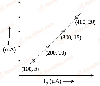
The transfer characteristic curve of a transistor, having input and output resistance 100 Ω and 100 kΩ respectively, is shown in the figure. The voltage and power gain, are respectively:

Figure for JEE Main 2019 Physics question on Transistors (older syllabus)
  1. A

    5×1045 \times 10^4, 2.5×1062.5 \times 10^6

  2. B

    2.5×1042.5 \times 10^4, 2.5×1062.5 \times 10^6

  3. C

    5×1045 \times 10^4, 5×1065 \times 10^6

  4. D

    5×1045 \times 10^4, 5×1055 \times 10^5

JEE MAIN 2018 · 15 APR S1Transistors (older syllabus)TRANSCRIBED

In a common emitter configuration with suitable bias, it is given than RLR_L is the load resistance and RBER_{BE} is small signal dynamic resistance (input side). Then, voltage gain, current gain and power gain are given, respectively, by: [β\beta is current gain, IBI_B, ICI_C, IEI_E are respectively base, collector and emitter currents]

  1. A

    βRLRBE,ΔIEΔIB,β2RLRBE\beta \frac{R_L}{R_{BE}}, \frac{\Delta I_E}{\Delta I_B}, \beta^2 \frac{R_L}{R_{BE}}

  2. B

    β2RLRBE,ΔICΔIB,βRLRBE\beta^2 \frac{R_L}{R_{BE}}, \frac{\Delta I_C}{\Delta I_B}, \beta \frac{R_L}{R_{BE}}

  3. C

    β2RLRBE,ΔICΔIE,β2RLRBE\beta^2 \frac{R_L}{R_{BE}}, \frac{\Delta I_C}{\Delta I_E}, \beta^2 \frac{R_L}{R_{BE}}

  4. D

    βRLRBE,ΔICΔIB,β2RLRBE\beta \frac{R_L}{R_{BE}}, \frac{\Delta I_C}{\Delta I_B}, \beta^2 \frac{R_L}{R_{BE}}

JEE MAIN 2018 · 08 APR OFFLINETransistors (older syllabus)TRANSCRIBED

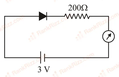
The reading of the ammeter for a silicon diode in the given circuit is:
Figure for JEE Main 2018 Physics question on Transistors (older syllabus)

  1. A

    13.5 mA

  2. B

    0

  3. C

    15 mA

  4. D

    11.5 mA

JEE MAIN 2017 · 02 APR OFFLINETransistors (older syllabus)TRANSCRIBED

In a common emitter amplifier circuit using an nn-pp-nn transistor, the phase difference between the input and the output voltages will be:

  1. A

    180°

  2. B

    45°

  3. C

    90°

  4. D

    135°

JEE MAIN 2017 · 09 APR ONLINETransistors (older syllabus)TRANSCRIBED

The current gain of a common emitter amplifier is 69. If the emitter current is 7.0 mA, collector current is:

  1. A

    69 mA

  2. B

    0.69 mA

  3. C

    6.9 mA

  4. D

    9.6 mA

JEE MAIN 2016 · 03 APR OFFLINETransistors (older syllabus)TRANSCRIBED

For a common emitter configuration, if α\alpha and β\beta have their usual meanings, the correct relationship between α\alpha and β\beta is:

  1. A

    α=β1+β\alpha = \frac{\beta}{1+\beta}

  2. B

    α=β21+β2\alpha = \frac{\beta^2}{1+\beta^2}

  3. C

    1α=1β−1\frac{1}{\alpha} = \frac{1}{\beta} - 1

  4. D

    α=β1−β\alpha = \frac{\beta}{1-\beta}

JEE MAIN 2016 · 09 APR ONLINETransistors (older syllabus)TRANSCRIBED

An unknown transistor needs to be identified as a npn or pnp type. A multimeter, with +ve and -ve terminals, is used to measure resistance between different terminals of transistor. If terminal 2 is the base of the transistor then which of the following is correct for a pnp transistor?

  1. A

    +ve terminal 2, -ve terminal 3, resistance low

  2. B

    +ve terminal 2, -ve terminal 1, resistance high

  3. C

    +ve terminal 1, -ve terminal 2, resistance high

  4. D

    +ve terminal 3, -ve terminal 2, resistance high

JEE MAIN 2016 · 10 APR ONLINETransistors (older syllabus)TRANSCRIBED

The ratio (R) of output resistance r0r_0, and the input resistance rir_i in measurements of input and output characteristics of a transistor is typically in the range:

  1. A

    R∼102−103R \sim 10^2 - 10^3

  2. B

    R∼1−10R \sim 1 - 10

  3. C

    R∼0.1−1.0R \sim 0.1 - 1.0

  4. D

    R∼0.1−0.01R \sim 0.1 - 0.01

JEE MAIN 2016 · 10 APR ONLINETransistors (older syllabus)TRANSCRIBED

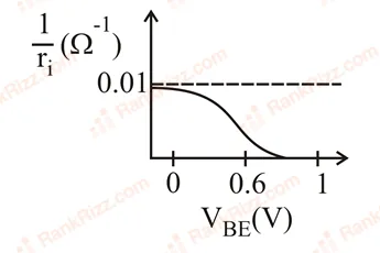
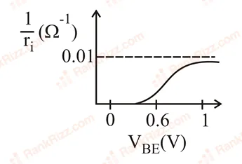
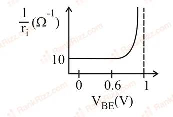
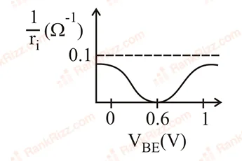
A realistic graph depicting the variation of the reciprocal of input resistance in an input characteristics measurement in a common emitter transistor configuration is:

  1. A
    Figure for JEE Main 2016 Physics question on Transistors (older syllabus)
  2. B
    Figure for JEE Main 2016 Physics question on Transistors (older syllabus)
  3. C
    Figure for JEE Main 2016 Physics question on Transistors (older syllabus)
  4. D
    Figure for JEE Main 2016 Physics question on Transistors (older syllabus)
JEE MAIN 2014 · 09 APR ONLINETransistors (older syllabus)TRANSCRIBED

An n-p-n transistor has three leads A, B and C. Connecting B and C by moist fingers, A to the positive lead of an ammeter, and C to the negative lead of the ammeter, one finds large deflection. Then, A, B and C refer respectively to:

  1. A

    Base, emitter and collector

  2. B

    Base, collector and emitter

  3. C

    Emitter, base and collector

  4. D

    Collector, emitter and base

JEE MAIN 2008Transistors (older syllabus)TRANSCRIBED

A working transistor with its three legs marked P,QP, Q and RR is tested using a multimeter. No conduction is found between PP and QQ. By connecting the common (negative) terminal of the multimeter to RR and the other (positive) terminal to PP or QQ, some resistance is seen on the multimeter. Which of the following is true for the transistor?

  1. A

    It is an npn transistor with RR as base

  2. B

    It is a pnp transistor with RR as collector

  3. C

    It is a pnp transistor with RR as emitter

  4. D

    It is an npn transistor with RR as collector

JEE MAIN 2006Transistors (older syllabus)TRANSCRIBED

In a common base mode of a transistor, the collector current is 5.488 mA5.488\,mA for an emitter current of 5.60 mA5.60\,mA. The value of the base current amplification factor (β)(\beta) will be

  1. A

    48

  2. B

    49

  3. C

    50

  4. D

    51

JEE MAIN 2005Transistors (older syllabus)TRANSCRIBED

In a common base amplifier, the phase difference between the input signal voltage and output voltage is

  1. A

    π4\frac{\pi}{4}

  2. B

    π\pi

  3. C

    00

  4. D

    π2\frac{\pi}{2}