RankRizz

p-n junction diode and its characteristics — JEE Main Previous Year Questions

Every JEE Main question on p-n junction diode and its characteristics, one of the ideas inside Semiconductor Electronics: 55 questions from 2004–2026, 29 of them in the last five years. Newest first, answer key on every one. Free to read.

Questions

55

Years asked

15

Since

2004

Of the chapter

22%

Every p-n junction diode and its characteristics question

21–40 OF 55 · NEWEST FIRST

JEE MAIN 2022 · 28 JUN S1p-n junction diode and its characteristicsTRANSCRIBED

For using a multimeter to identify diode from electrical components, choose the correct statement out of the following about the diode

  1. A

    It is two terminal device which conducts current in both directions.

  2. B

    It is two terminal device which conducts current in one direction only

  3. C

    It does not conduct current gives an initial deflection which decays to zero.

  4. D

    It is three terminal device which conducts current in one direction only between central terminal and either of the remaining two terminals
JEE MAIN 2022 · 26 JUN S1p-n junction diode and its characteristicsTRANSCRIBED

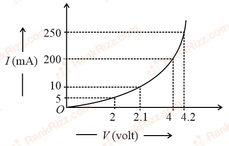
The I - V characteristics of a p−np - n junction diode in forward bias is shown in the figure. The ratio of dynamic resistance, corresponding to forward bias voltage of 22 V and 44 V respective isFigure for JEE Main 2022 Physics question on p-n junction diode and its characteristics

  1. A

    1:21 : 2

  2. B

    5:15 : 1

  3. C

    1:401 : 40

  4. D

    20:120 : 1

JEE MAIN 2022 · 28 JUN S2p-n junction diode and its characteristicsTRANSCRIBED

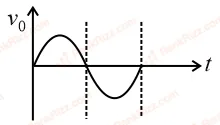
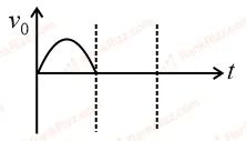
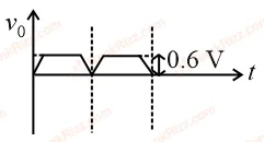
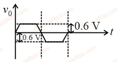
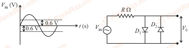
In the given circuit the input voltage VinV_{in} is shown in figure. The cut-in voltage of p−np-n junction diode (D1D_1 or D2D_2) is 0.6 V. Which of the following output voltage (V0V_0) waveform across the diode is correct?

Figure for JEE Main 2022 Physics question on p-n junction diode and its characteristics
  1. A
    Figure for JEE Main 2022 Physics question on p-n junction diode and its characteristics
  2. B
    Figure for JEE Main 2022 Physics question on p-n junction diode and its characteristics
  3. C
    Figure for JEE Main 2022 Physics question on p-n junction diode and its characteristics
  4. D
    Figure for JEE Main 2022 Physics question on p-n junction diode and its characteristics
JEE MAIN 2022 · 24 JUN S2p-n junction diode and its characteristicsTRANSCRIBED

In the given circuit, the value of current ILI_L will be ______ mA. (When RL=1R_L = 1 kΩ\Omega)

Figure for JEE Main 2022 Physics question on p-n junction diode and its characteristics
JEE MAIN 2022 · 26 JUN S1p-n junction diode and its characteristicsTRANSCRIBED

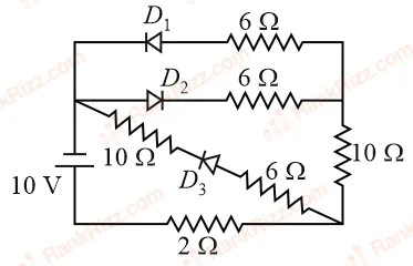
As per the given circuit, the value of current through the battery will be ______ A.Figure for JEE Main 2022 Physics question on p-n junction diode and its characteristics

JEE MAIN 2022 · 29 JUN S2p-n junction diode and its characteristicsTRANSCRIBED

A potential barrier of 0.4 V exists across a p-n junction. An electron enters the junction from the nn-side with a speed of 6.0×1056.0 \times 10^5 m s−1^{-1}. The speed with which electron enters the pp side will be x3×105\frac{x}{3} \times 10^5 m s−1^{-1}, then the value of xx is ______.: (Given mass of electron =9×10−31= 9 \times 10^{-31} kg, charge on electron =1.6×10−19= 1.6 \times 10^{-19} C.)

JEE MAIN 2022 · 27 JUN S2p-n junction diode and its characteristicsTRANSCRIBED

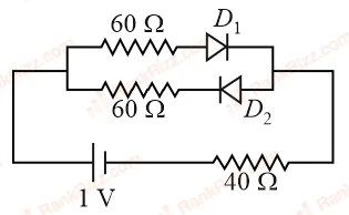
The cut-off voltage of the diodes (shown in figure) in forward bias is 0.60.6 V. The current through the resister of 40Ω40\Omega is ______ mA.

Figure for JEE Main 2022 Physics question on p-n junction diode and its characteristics
JEE MAIN 2022 · 25 JUL S2p-n junction diode and its characteristicsTRANSCRIBED

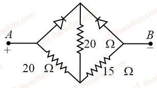
Two ideal diodes are connected in the network as shown in figure. The equivalent resistance between AA and BB is ______ Ω\Omega.

Figure for JEE Main 2022 Physics question on p-n junction diode and its characteristics
JEE MAIN 2022 · 29 JUL S1p-n junction diode and its characteristicsTRANSCRIBED

If the potential barrier across a p-n junction is 0.6 V. Then the electric field intensity, in the depletion region having the width of 6×10−66 \times 10^{-6} m, will be _____ ×105\times 10^5 N C−1^{-1}

JEE MAIN 2021 · 25 FEB S1p-n junction diode and its characteristicsTRANSCRIBED

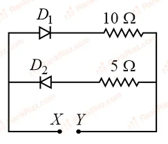
A 5 V battery is connected across the points X and Y. Assume D1D_1 and D2D_2 to be normal silicon diodes. Find the current supplied by the battery if the +ve terminal of the battery is connected to point X.

Figure for JEE Main 2021 Physics question on p-n junction diode and its characteristics
  1. A

    ~0.86 A

  2. B

    ~0.5 A

  3. C

    ~1.5 A

  4. D

    ~0.43 A

JEE MAIN 2021 · 31 AUG S1p-n junction diode and its characteristicsTRANSCRIBED

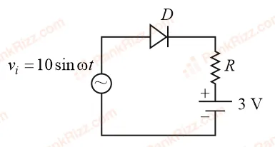
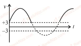
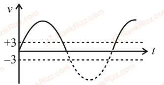
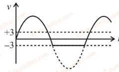
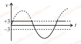
Choose the correct waveform that can represent the voltage across RR of the following circuit, assuming the diode is ideal one:

Figure for JEE Main 2021 Physics question on p-n junction diode and its characteristics
  1. A
    Figure for JEE Main 2021 Physics question on p-n junction diode and its characteristics
  2. B
    Figure for JEE Main 2021 Physics question on p-n junction diode and its characteristics
  3. C
    Figure for JEE Main 2021 Physics question on p-n junction diode and its characteristics
  4. D
    Figure for JEE Main 2021 Physics question on p-n junction diode and its characteristics
JEE MAIN 2021 · 25 FEB S2p-n junction diode and its characteristicsTRANSCRIBED

For extrinsic semiconductors; when doping level is increased;

  1. A

    Fermi-level of pp and nn-type semiconductors will not be affected.

  2. B

    Fermi-level of pp-type semiconductor will go upward and Fermi-level of nn-type semiconductors will go downward.

  3. C

    Fermi-level of both p-type and n-type semiconductors will go upward for T>TFT > T_F K and downward for T<TFT < T_F K, where TFT_F is Fermi temperature.

  4. D

    Fermi-level of pp-type semiconductors will go downward and Fermi-level of nn-type semiconductor will go upward.

JEE MAIN 2021 · 26 AUG S1p-n junction diode and its characteristicsTRANSCRIBED

Statement I: By doping silicon semiconductors with pentavalent material, the electrons density increases.
Statement II: The n-type of semiconductor has a net negative charge.
In the above statements, choose the most appropriate answer from the options given below:

  1. A

    Both Statement I and Statement II are false.

  2. B

    Statement I is true but Statement II is false.

  3. C

    Statement I is false but Statement II is true.

  4. D

    Both Statement I and Statement II are true.

JEE MAIN 2021 · 22 JUL S1p-n junction diode and its characteristicsTRANSCRIBED

Consider a situation in which reverse biased current of a particular P-N junction increases when it is exposed to a light of wavelength ≤\le 621 nm. During this process, enhancement in carrier concentration takes place due to generation of hole-electron pairs. The value of band gap is nearly.

  1. A

    2 eV

  2. B

    4 eV

  3. C

    1 eV

  4. D

    0.5 eV

JEE MAIN 2021 · 20 JUL S1p-n junction diode and its characteristicsTRANSCRIBED

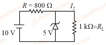
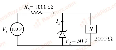
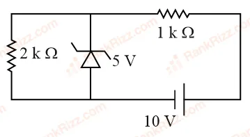
For the circuit shown below, calculate the value of IzI_z:

Figure for JEE Main 2021 Physics question on p-n junction diode and its characteristics
  1. A

    25 mA

  2. B

    0.15 A

  3. C

    0.1 A

  4. D

    0.05 A

JEE MAIN 2021 · 31 AUG S2p-n junction diode and its characteristicsTRANSCRIBED

Statement I: To get a steady DC output from the pulsating voltage received from a full wave rectifier we can connect a capacitor across the output parallel to the load RLR_L.
Statement II: To get a steady DC output from the pulsating voltage received from a full wave rectifier we can connect an inductor in series with RLR_L.
In the light of the above statements, choose the most appropriate answer from the options given below:

  1. A

    Both Statement I and Statement II are false

  2. B

    Both Statement I and Statement II are true

  3. C

    Statement I is false but Statement II is true

  4. D

    Statement I is true but Statement II is false

JEE MAIN 2021 · 01 SEP S2p-n junction diode and its characteristicsTRANSCRIBED

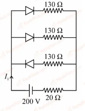
In the given figure, each diode has a forward bias resistance of 30 Ω\Omega and infinite resistance in reverse bias. The current I1I_1 will be:

Figure for JEE Main 2021 Physics question on p-n junction diode and its characteristics
  1. A

    2.0 A

  2. B

    3.75 A

  3. C

    2.73 A

  4. D

    2.35 A

JEE MAIN 2021 · 25 JUL S2p-n junction diode and its characteristicsTRANSCRIBED

In a semiconductor, the number density of intrinsic charge carriers at 27°C is 1.5×10161.5 \times 10^{16} m−3^{-3}. If the semiconductor is doped with an impurity atom, the hole density increases to 4.5×10224.5 \times 10^{22} m−3^{-3}. The electron density in the doped semiconductor is _________ ×109\times 10^{9} m−3^{-3}

JEE MAIN 2021 · 24 FEB S1p-n junction diode and its characteristicsTRANSCRIBED

In connection with the circuit drawn below, the value of current flowing through 2 kΩ\Omega resistor is ______ ×10−4\times 10^{-4} A.

Figure for JEE Main 2021 Physics question on p-n junction diode and its characteristics
JEE MAIN 2021 · 20 JUL S2p-n junction diode and its characteristicsTRANSCRIBED

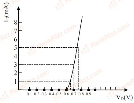
For the forward biased diode characteristics shown in the figure, the dynamic resistance at ID=3I_D = 3 mA will be ___ Ω\Omega.

Figure for JEE Main 2021 Physics question on p-n junction diode and its characteristics