RankRizz

p-n junction diode and its characteristics — JEE Main Previous Year Questions

Every JEE Main question on p-n junction diode and its characteristics, one of the ideas inside Semiconductor Electronics: 55 questions from 2004–2026, 29 of them in the last five years. Newest first, answer key on every one. Free to read.

Questions

55

Years asked

15

Since

2004

Of the chapter

22%

Every p-n junction diode and its characteristics question

41–55 OF 55 · NEWEST FIRST

JEE MAIN 2020 · 03 SEP S2p-n junction diode and its characteristicsTRANSCRIBED

Which of the following will NOT be observed when a multimeter (operating in resistance measuring mode) probes connected across a component, are just reversed?

  1. A

    Multimeter shows an equal deflection in both cases i.e., before and after reversing the probes if the chosen component is resistor

  2. B

    Multimeter shows NO deflection in both cases i.e. before and after reversing the probes if the chosen component is capacitor

  3. C

    Multimeter shows a deflection, accompanied by a splash of light out of connected component in one direction and NO deflection on reversing the probes if the chosen component is LED

  4. D

    Multimeter shows NO deflection in both cases i.e. before and after reversing the probes is the chosen component is metal wire.
JEE MAIN 2020 · 03 SEP S1p-n junction diode and its characteristicsTRANSCRIBED

When a diode is forward biased, it has a voltage drop of 0.5 V. The safe limit of current through the diode is 10 mA. If a battery of emf 1.5 V is used in the circuit, the value of minimum resistance to be connected in series with the diode so that the current does not exceed the safe limit is:

  1. A

    300 Ω\Omega

  2. B

    50 Ω\Omega

  3. C

    100 Ω\Omega

  4. D

    200 Ω\Omega

JEE MAIN 2020 · 09 JAN S1p-n junction diode and its characteristicsTRANSCRIBED

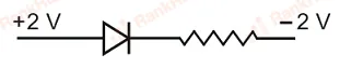
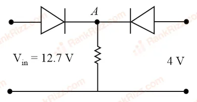
Both the diodes used in the circuit shown are assumed to be ideal and have negligible resistance when these are forward biased. Built in potential in each diode is 0.7V0.7V. For the input voltages shown in the figure, the voltage (in Volts) at point A is ___________.

Figure for JEE Main 2020 Physics question on p-n junction diode and its characteristics
JEE MAIN 2019 · 09 JAN S1p-n junction diode and its characteristicsTRANSCRIBED

Mobility of electrons in a semiconductor is defined as the ratio of their drift velocity to the applied electric field. If, for an N-type semiconductor, the density of electrons is 101910^{19} m−3^{-3} and their mobility is 1.6 m2^2 V−1^{-1} s−1^{-1}, then the resistivity of the semiconductor (since it is an N-type semiconductor contribution of holes is ignored) is close to:

  1. A

    0.2 Ω\Omega m

  2. B

    4 Ω\Omega m

  3. C

    2 Ω\Omega m

  4. D

    0.4 Ω\Omega m

JEE MAIN 2019 · 09 JAN S2p-n junction diode and its characteristicsTRANSCRIBED

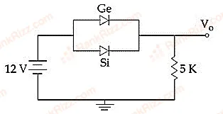
Ge and Si diodes start conducting at 0.3 V and 0.7 V respectively. In the following figure if Ge diode connection are reversed, the value of V0V_0 changes by: (assume that the Ge diode has large breakdown voltage)

Figure for JEE Main 2019 Physics question on p-n junction diode and its characteristics
  1. A

    0.8 V

  2. B

    0.4 V

  3. C

    0.2 V

  4. D

    0.6 V

JEE MAIN 2019 · 11 JAN S2p-n junction diode and its characteristicsTRANSCRIBED

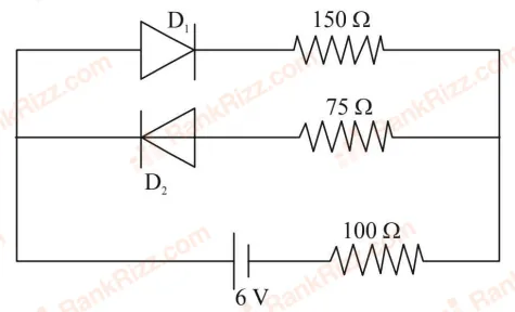
The circuit shown below contains two ideal diodes, each with a forward resistance of 50Ω50\Omega. If the battery voltage is 6 V, the current through the 100Ω100\Omega resistance (in Amperes) is:

Figure for JEE Main 2019 Physics question on p-n junction diode and its characteristics
  1. A

    0.036

  2. B

    0.02

  3. C

    0.027

  4. D

    0.03

JEE MAIN 2017 · 08 APR ONLINEp-n junction diode and its characteristicsTRANSCRIBED

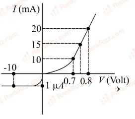
The V−IV - I characteristic of a diode is shown in the figure. The ratio of forward to reverse bias resistance is:

Figure for JEE Main 2017 Physics question on p-n junction diode and its characteristics
  1. A

    100

  2. B

    10610^6

  3. C

    10−610^{-6}

  4. D

    10

JEE MAIN 2017 · 08 APR ONLINEp-n junction diode and its characteristicsTRANSCRIBED

The conductivity of a semiconductor sample having electron concentration of 5×10185 \times 10^{18} electrons m−3^{-3}, hole concentration of 5×10195 \times 10^{19} holes m−3^{-3}, electron mobility of 2.0 m2^2 V−1^{-1} s−1^{-1} and hole mobility of 0.01 m2^2 V−1^{-1} s−1^{-1} is: (Take charge of an electron as 1.6×10−191.6 \times 10^{-19} C)

  1. A

    1.83 (Ω m)−1(\Omega \text{ m})^{-1}

  2. B

    1.65 (Ω m)−1(\Omega \text{ m})^{-1}

  3. C

    1.20 (Ω m)−1(\Omega \text{ m})^{-1}

  4. D

    0.59 (Ω m)−1(\Omega \text{ m})^{-1}

JEE MAIN 2016 · 03 APR OFFLINEp-n junction diode and its characteristicsTRANSCRIBED

The temperature dependence of resistance of Cu and undoped Si in the temperature range 300 - 400 K is best described by:

  1. A

    linear increase for Cu, exponential decrease for Si

  2. B

    linear decrease for Cu, linear decrease for Si

  3. C

    linear increase for Cu, linear increase for Si

  4. D

    linear increase for Cu, exponential increase for Si

JEE MAIN 2015 · 10 APR ONLINEp-n junction diode and its characteristicsTRANSCRIBED

In an unbiased p - n junction electrons diffuse from n-region to p-region because:

  1. A

    electrons travel across the junction due to potential difference

  2. B

    only electrons move from n to p region and not the vice - versa

  3. C

    electron concentration in n - region is more as compared to that in p - region

  4. D

    holes in p - region attract them

JEE MAIN 2014 · 06 APR OFFLINEp-n junction diode and its characteristicsTRANSCRIBED

The current voltage relation of diode is given by I=(e1000V/T−1)I = (e^{1000V/T} - 1) mA, where the applied voltage V is in volts and the temperature T is in degree Kelvin. If a student makes an error measuring ±0.01\pm 0.01 V while measuring the current of 5 mA at 300 K, what will be the error in the value of current in mA?

  1. A

    0.2 mA

  2. B

    0.02 mA

  3. C

    0.5 mA

  4. D

    0.05 mA

JEE MAIN 2014 · 06 APR OFFLINEp-n junction diode and its characteristicsTRANSCRIBED

The forward biased diode connection is:

  1. A
    Figure for JEE Main 2014 Physics question on p-n junction diode and its characteristics
  2. B
    Figure for JEE Main 2014 Physics question on p-n junction diode and its characteristics
  3. C
    Figure for JEE Main 2014 Physics question on p-n junction diode and its characteristics
  4. D
    Figure for JEE Main 2014 Physics question on p-n junction diode and its characteristics
JEE MAIN 2013 · 22 APR ONLINEp-n junction diode and its characteristicsTRANSCRIBED

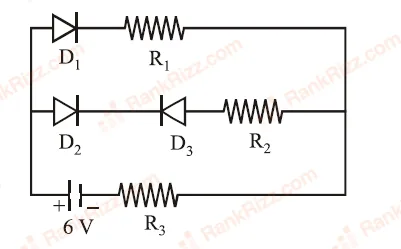
Figure shows a circuit in which three identical diodes are used. Each diode has forward resistance of 20Ω\Omega and infinite backward resistance. Resistors R1=R2=R3=50ΩR_1 = R_2 = R_3 = 50\Omega. Battery voltage is 6 V. The current through R3R_3 is :

Figure for JEE Main 2013 Physics question on p-n junction diode and its characteristics
  1. A

    50 mA

  2. B

    100 mA

  3. C

    60 mA

  4. D

    25 mA

JEE MAIN 2006p-n junction diode and its characteristicsTRANSCRIBED

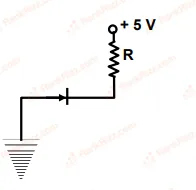
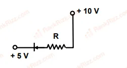
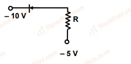
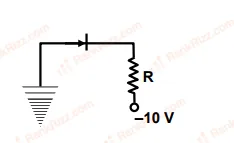
In the following, which one of the diodes is reverse biased?

  1. A
    Figure for JEE Main 2006 Physics question on p-n junction diode and its characteristics
  2. B
    Figure for JEE Main 2006 Physics question on p-n junction diode and its characteristics
  3. C
    Figure for JEE Main 2006 Physics question on p-n junction diode and its characteristics
  4. D
    Figure for JEE Main 2006 Physics question on p-n junction diode and its characteristics
JEE MAIN 2004p-n junction diode and its characteristicsTRANSCRIBED

When p-n junction diode is forward biased

  1. A

    the depletion region is reduced and barrier height is increased

  2. B

    the depletion region is widened and barrier height is reduced

  3. C

    both the depletion region and barrier height reduced

  4. D

    both the depletion region and barrier height increased