JEE Main 2026 Physics question — p-n junction diode and its characteristics
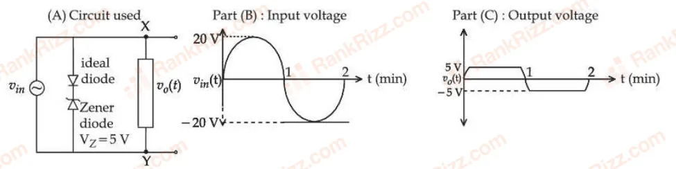
For the given circuit (shown in part (A)) the time dependent input voltage and corresponding output are shown in part (B) and part (C), respectively. Identify the components that are used in the circuit between points X and Y.
SOLUTION
The input waveform shown in part (B) is an undistorted sinusoid that swings symmetrically above and below the 0-V axis.
The output waveform shown in part (C) is identical to the positive half-cycles of the input, whereas the entire negative half-cycles are missing (the output remains at 0 V whenever the input is negative).
This behaviour is the signature of an ideal half-wave rectifier:
• During the positive half-cycle, the rectifying element is forward-biased, it conducts, and (neglecting the small forward drop).
• During the negative half-cycle, the rectifying element is reverse-biased, it blocks, and the load sees no current, so .
The simplest circuit that realises a half-wave rectifier between the points X (input node) and Y (output node) is a single p-n diode (anode at X, cathode at Y) feeding a load resistor connected from Y to ground. No other passive component can reproduce exactly this “positive-half-only” transfer characteristic.
Hence the network between X and Y must consist of a forward-biased diode in series with the load, i.e. the arrangement given in Option A.
Option A which is: a single diode (anode at X, cathode at Y) forming a half-wave rectifier.
Tagged p-n junction diode and its characteristics. Machine-assigned, so read it as a strong shortlist rather than a verdict.