RankRizzStart free

Semiconductor Electronics — JEE Main Previous Year Questions

Every Semiconductor Electronics question JEE Main has set, grouped by the idea it tests rather than the order of the syllabus. 253 questions across 5 distinct ideas. Free to read, answer key on every one.

Questions

253

Distinct ideas

5

Share of marks

4.4%

Difficulty

EASY

The ideas inside Semiconductor Electronics

A chapter is not one subject — it is a handful of procedures the examiner reuses. These are the ones Semiconductor Electronics questions actually test.

01Semiconductors: energy bands, intrinsic and extrinsicset 9×
02p-n junction diode and its characteristicsset 102×
03Diode circuits and rectifiersset 14×
04Zener diode, LED, photodiode and solar cellPractice questions coming soon
05Logic gates and digital circuitsset 85×
06Transistors (older syllabus)set 43×

Every Semiconductor Electronics question

161–180 OF 253 · NEWEST FIRST

JEE MAIN 2020 · 03 SEP S2p-n junction diode and its characteristicsTRANSCRIBED

Which of the following will NOT be observed when a multimeter (operating in resistance measuring mode) probes connected across a component, are just reversed?

  1. A

    Multimeter shows an equal deflection in both cases i.e., before and after reversing the probes if the chosen component is resistor

  2. B

    Multimeter shows NO deflection in both cases i.e. before and after reversing the probes if the chosen component is capacitor

  3. C

    Multimeter shows a deflection, accompanied by a splash of light out of connected component in one direction and NO deflection on reversing the probes if the chosen component is LED

  4. D

    Multimeter shows NO deflection in both cases i.e. before and after reversing the probes is the chosen component is metal wire.
JEE MAIN 2020 · 03 SEP S1p-n junction diode and its characteristicsTRANSCRIBED

When a diode is forward biased, it has a voltage drop of 0.5 V. The safe limit of current through the diode is 10 mA. If a battery of emf 1.5 V is used in the circuit, the value of minimum resistance to be connected in series with the diode so that the current does not exceed the safe limit is:

  1. A

    300

  2. B

    50

  3. C

    100

  4. D

    200

JEE MAIN 2020 · 06 SEP S1Logic gates and digital circuitsTRANSCRIBED

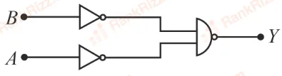
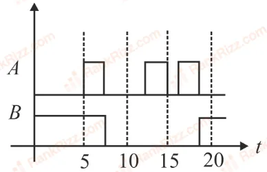
Identify the correct output signal in the given combination of gates (as shown ) for the given inputs and :

imageimage
  1. A
    image
  2. B
    image
  3. C
    image
  4. D
    image
JEE MAIN 2020 · 07 JAN S1Logic gates and digital circuitsTRANSCRIBED

Which of the following gives a reversible operation?

  1. A
    image
  2. B
    image
  3. C
    image
  4. D
    image
JEE MAIN 2020 · 05 SEP S1p-n junction diode and its characteristicsTRANSCRIBED

With increasing biasing voltage of a photo diode, the photocurrent magnitude:

  1. A

    remains constant

  2. B

    increases initially and after attaining certain value, it decreases

  3. C

    increases linearly

  4. D

    increases initially and saturates finally

JEE MAIN 2020 · 09 JAN S2Diode circuits and rectifiersTRANSCRIBED

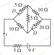
The current in the network is:

  1. A

    0.2 A

  2. B

    0.6 A

  3. C

    0.3 A

  4. D

    0 A

JEE MAIN 2020 · 05 SEP S2p-n junction diode and its characteristicsTRANSCRIBED

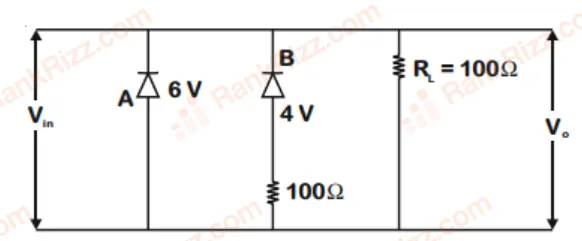
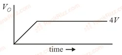
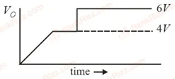
Two Zener diodes ( and ) having breakdown voltages of and respectively, are connected as shown in the circuit below. The output voltage variation with input voltage linearly increasing with time, is given by ( at ):

image
  1. A
  2. B
  3. C
  4. D
JEE MAIN 2020 · 03 SEP S2p-n junction diode and its characteristicsTRANSCRIBED

If a semiconductor photo diode can detect a photon with a maximum wavelength of 400 nm, then its band gap energy is: Planck's constant h = 6.63 10 J.s, Speed of light c = 3 10 m s

  1. A

    1.1 eV

  2. B

    2.0 eV

  3. C

    1.5 eV

  4. D

    3.1 eV

JEE MAIN 2020 · 04 SEP S1p-n junction diode and its characteristicsTRANSCRIBED

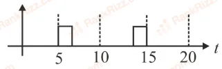
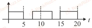
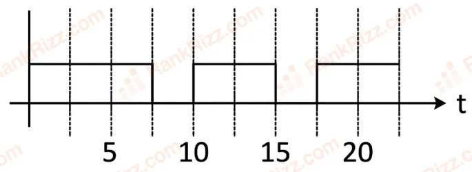
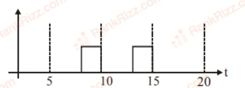
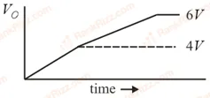
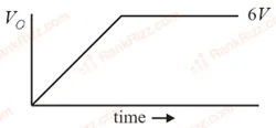
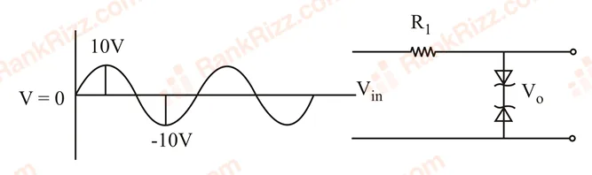
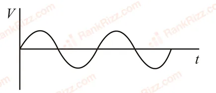
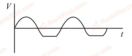
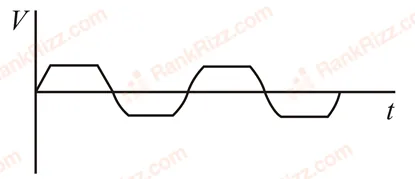
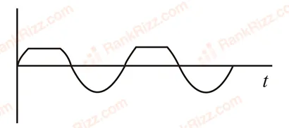
Take the breakdown voltage of the zener diode used in the given circuit as 6V. For the input voltage shown in the figure below, the time variation of the output voltage is: (Graphs drawn are schematic and not to the scale)

  1. A
    image
  2. B
    image
  3. C
    image
  4. D
    image
JEE MAIN 2020 · 08 JAN S1Logic gates and digital circuitsTRANSCRIBED

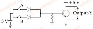
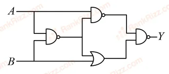
Boolean relation at the output stage Y for the following circuit is:

  1. A

  2. B

  3. C

  4. D

JEE MAIN 2020 · 02 SEP S2Logic gates and digital circuitsTRANSCRIBED

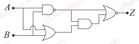
In the following digital circuit, what will be the output 'Z', when the input (A, B) are (1, 0), (0, 0), (1, 1), (0, 1):

  1. A

    0, 0, 1, 0

  2. B

    1, 0, 1, 1

  3. C

    1, 1, 0, 1

  4. D

    0, 1, 0, 0

JEE MAIN 2020 · 04 SEP S2Logic gates and digital circuitsTRANSCRIBED

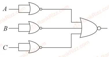
Identify the operation performed by the circuit given below:

  1. A

    NAND

  2. B

    OR

  3. C

    AND

  4. D

    NOT

JEE MAIN 2020 · 08 JAN S2Logic gates and digital circuitsTRANSCRIBED

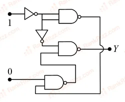
In the given circuit, value of Y is:

  1. A

    0

  2. B

    toggles between 0 and 1

  3. C

    will not execute

  4. D

    1

JEE MAIN 2020 · 09 JAN S1p-n junction diode and its characteristicsTRANSCRIBED

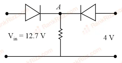
Both the diodes used in the circuit shown are assumed to be ideal and have negligible resistance when these are forward biased. Built in potential in each diode is . For the input voltages shown in the figure, the voltage (in Volts) at point A is ___________.

JEE MAIN 2020 · 09 JAN S2p-n junction diode and its characteristicsTRANSCRIBED

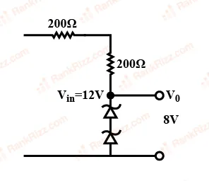
In the circuit shown below, is working as a 8 V dc regulated voltage source. When 12 V is used as an input, the power dissipated (in mW) in each diode is (Considering both zener diodes are identical) ___________.

JEE MAIN 2020 · 06 SEP S2Transistors (older syllabus)TRANSCRIBED

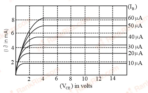
The output characteristics of a transistor is shown in the figure. When is and , then value of is___

JEE MAIN 2019 · 09 JAN S1p-n junction diode and its characteristicsTRANSCRIBED

Mobility of electrons in a semiconductor is defined as the ratio of their drift velocity to the applied electric field. If, for an N-type semiconductor, the density of electrons is m and their mobility is 1.6 m V s, then the resistivity of the semiconductor (since it is an N-type semiconductor contribution of holes is ignored) is close to:

  1. A

    0.2 m

  2. B

    4 m

  3. C

    2 m

  4. D

    0.4 m

JEE MAIN 2019 · 12 JAN S1Logic gates and digital circuitsTRANSCRIBED

The output of the given logic circuit is:

  1. A

  2. B

  3. C

  4. D

JEE MAIN 2019 · 11 JAN S1p-n junction diode and its characteristicsTRANSCRIBED

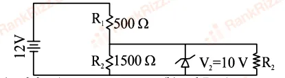
In the given circuit the current through Zener Diode is close to:

  1. A

    0.0 mA

  2. B

    6.7 mA

  3. C

    4.0 mA

  4. D

    6.0 mA

JEE MAIN 2019 · 10 APR S1Transistors (older syllabus)TRANSCRIBED

An NPN transistor operates as a common emitter amplifier, with a power gain of 60 dB. The input circuit resistance is 100 Ω and the output load resistance is 10 kΩ. The common emitter current gain β is:

  1. A

  2. B

  3. C

  4. D

    60