JEE MAIN 2021 · 20 JUL S1p-n junction diode and its characteristicsTRANSCRIBED
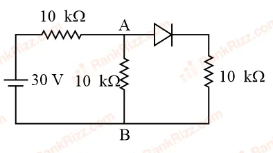
For the circuit shown below, calculate the value of :
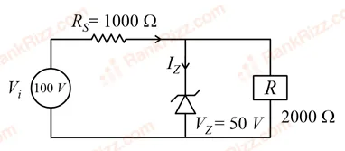
- A
25 mA
- B
0.15 A
- C
0.1 A
- D
0.05 A
Every Semiconductor Electronics question JEE Main has set, grouped by the idea it tests rather than the order of the syllabus. 253 questions across 5 distinct ideas. Free to read, answer key on every one.
Questions
253
Distinct ideas
5
Share of marks
4.4%
Difficulty
EASY
A chapter is not one subject — it is a handful of procedures the examiner reuses. These are the ones Semiconductor Electronics questions actually test.
141–160 OF 253 · NEWEST FIRST
For the circuit shown below, calculate the value of :
25 mA
0.15 A
0.1 A
0.05 A
In the following logic circuit the sequence of the inputs , are and . The output for this sequence will be:
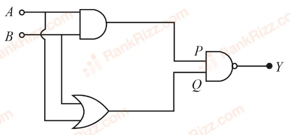
0, 1, 0, 1
0, 0, 1, 1
1, 1, 1, 0
1, 0, 1, 0
Find the truth table for the function Y of A and B represented in the following figure.
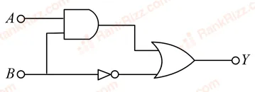
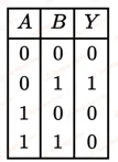
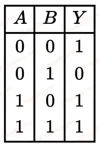
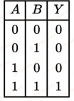
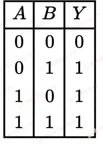
Statement I: To get a steady DC output from the pulsating voltage received from a full wave rectifier we can connect a capacitor across the output parallel to the load .
Statement II: To get a steady DC output from the pulsating voltage received from a full wave rectifier we can connect an inductor in series with .
In the light of the above statements, choose the most appropriate answer from the options given below:
Both Statement I and Statement II are false
Both Statement I and Statement II are true
Statement I is false but Statement II is true
Statement I is true but Statement II is false
In the given figure, each diode has a forward bias resistance of 30 and infinite resistance in reverse bias. The current will be:
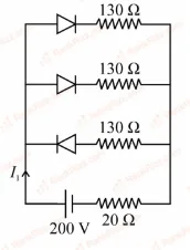
2.0 A
3.75 A
2.73 A
2.35 A
Draw the output signal Y in the given combination of gates.
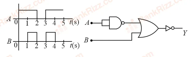
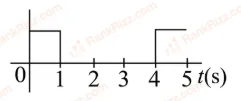
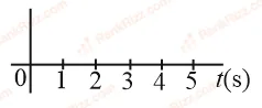
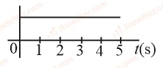
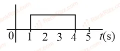
In a semiconductor, the number density of intrinsic charge carriers at 27°C is m. If the semiconductor is doped with an impurity atom, the hole density increases to m. The electron density in the doped semiconductor is _________ m
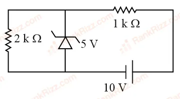
In connection with the circuit drawn below, the value of current flowing through 2 k resistor is ______ A.
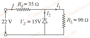
The value of power dissipated across the zener diode ( V) connected in the circuit as shown in the figure is W.
The value of to the nearest integer is ________.
The typical output characteristics curve for a transistor working in the common-emitter configuration is shown in the figure.
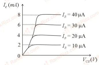
The estimated current gain from the figure is ___.
A circuit is arranged as shown in figure. The output voltage is equal to _________ V.
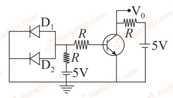
A transistor is connected in common emitter circuit configuration, the collector supply voltage is 10 V and the voltage drop across a resistor of 1000 in the collector circuit is 0.6 V. If the current gain factor is 24, then the base current is _________ A. (Round off to the Nearest Integer)
A zener diode having zener voltage 8 V and power dissipation rating of 0.5 W is connected across a potential divider arranged with maximum potential drop across zener diode as shown in the diagram. The value of protective resistance is ___ .
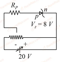
The zener diode has a V. The current passing through the diode for the following circuit is ______ mA.
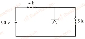
In the logic circuit shown in the figure, if input and are 0 to 1 respectively, the output at would be . The value of is ________.
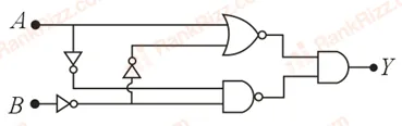
A zener diode of power rating 2 W is to be used as a voltage regulator. If the zener diode has a breakdown of 10 V and it has to regulate voltage fluctuated between 6 V and 14 V, the value of for safe operation should be _________ .
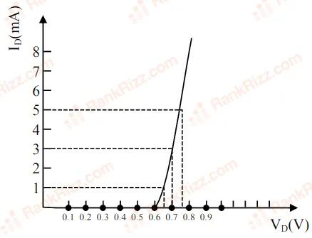
For the forward biased diode characteristics shown in the figure, the dynamic resistance at mA will be ___ .
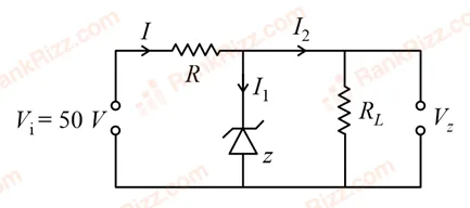
In a given circuit diagram, a 5 V zener diode along with a series resistance is connected across a 50 V power supply. The minimum value of the resistance required, if the maximum zener current is 90 mA will be ___ .
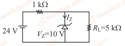
For the given circuit, the power across zener diode is _________ mW.
In the figure, potential difference between A and B is:
10 V
5 V
15 V
0 V
OTHER PHYSICS CHAPTERS