JEE MAIN 2021 · 24 FEB S2Logic gates and digital circuitsTRANSCRIBED
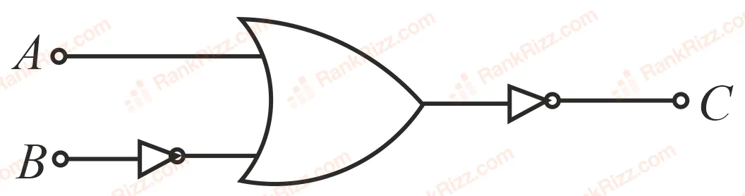
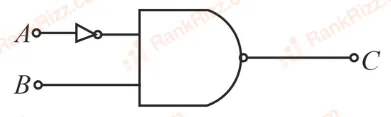
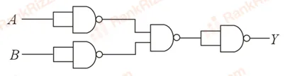
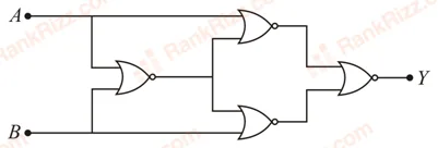
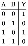
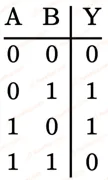
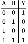
The logic circuit shown above is equivalent to:
- A
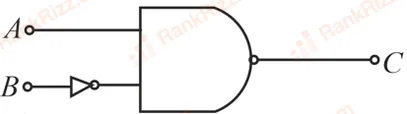
- B
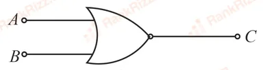
- C
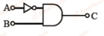
- D
Every Semiconductor Electronics question JEE Main has set, grouped by the idea it tests rather than the order of the syllabus. 253 questions across 5 distinct ideas. Free to read, answer key on every one.
Questions
253
Distinct ideas
5
Share of marks
4.4%
Difficulty
EASY
A chapter is not one subject — it is a handful of procedures the examiner reuses. These are the ones Semiconductor Electronics questions actually test.
121–140 OF 253 · NEWEST FIRST
The logic circuit shown above is equivalent to:
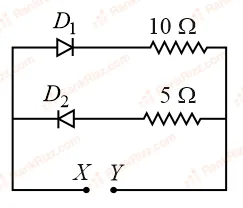
A 5 V battery is connected across the points X and Y. Assume and to be normal silicon diodes. Find the current supplied by the battery if the +ve terminal of the battery is connected to point X.
~0.86 A
~0.5 A
~1.5 A
~0.43 A
The truth table for the following logic circuit is:
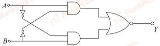
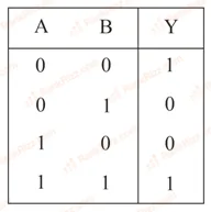
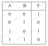
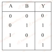
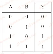
Identify the logic operation carried out by the given circuit:
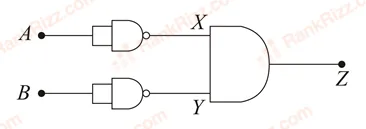
OR
AND
NAND
NOR
Zener breakdown occurs in a junction having and both:
lightly doped and have narrow depletion layer.
heavily doped and have wide depletion layer.
lightly doped and have wide depletion layer.
heavily doped and have narrow depletion layer.
For a transistor and are given as and . Then the correct relation between and will be:
The following logic gate is equivalent to:
NOR Gate
OR Gate
AND Gate
NAND Gate
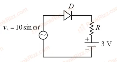
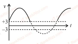
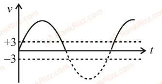
Choose the correct waveform that can represent the voltage across of the following circuit, assuming the diode is ideal one:
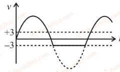
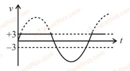
The output of the given combination gates represents:
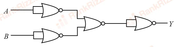
XOR Gate
NAND Gate
AND Gate
NOR Gate
For extrinsic semiconductors; when doping level is increased;
Fermi-level of and -type semiconductors will not be affected.
Fermi-level of -type semiconductor will go upward and Fermi-level of -type semiconductors will go downward.
Fermi-level of both p-type and n-type semiconductors will go upward for T > T_F K and downward for T < T_F K, where is Fermi temperature.
Fermi-level of -type semiconductors will go downward and Fermi-level of -type semiconductor will go upward.
If and are the input voltages (either 5 V or 0 V) and is the output voltage then the two gates represented in the following circuits A and B are:
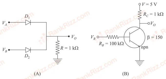
OR and NOT Gate
AND and NOT Gate
AND and OR Gate
NAND and NOR Gate
Statement I: By doping silicon semiconductors with pentavalent material, the electrons density increases.
Statement II: The n-type of semiconductor has a net negative charge.
In the above statements, choose the most appropriate answer from the options given below:
Both Statement I and Statement II are false.
Statement I is true but Statement II is false.
Statement I is false but Statement II is true.
Both Statement I and Statement II are true.
Which one of the following will be the output of the given circuit?

NOR Gate
NAND Gate
AND Gate
XOR Gate
Consider a situation in which reverse biased current of a particular P-N junction increases when it is exposed to a light of wavelength 621 nm. During this process, enhancement in carrier concentration takes place due to generation of hole-electron pairs. The value of band gap is nearly.
2 eV
4 eV
1 eV
0.5 eV
Four NOR gates are connected as shown in figure. The truth table for the given figure is:
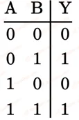
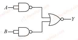
Identify the logic operation carried out.
OR
AND
NOR
NAND
If an emitter current is changed by 4 mA, the collector current changes by 3.5 mA. The value of will be:
3.5
0.5
0.875
7
The correct relation between (ratio of collector current to emitter current) and (ratio of collector current to base current) of a transistor is :
For a transistor in CE mode to be used as an amplifier, it must be operated in:
Cut-off region only
Saturation region only
The active region only
Both cut-off and Saturation
Given below are two statements:
Statement I: junction diodes can be used to function as a transistor, simply by connecting two diodes, back to back, which acts as the base terminal.
Statement II: In the study of transistors, the amplification factor indicates ratio of the collector current to the base current.
In the light of the above statements, choose the correct answer from the options given below.
Both Statement I and Statement II are false
Statement I is true but Statement II is false
Statement I is false but Statement II is true
Both Statement I and Statement II are true
OTHER PHYSICS CHAPTERS