JEE MAIN 2020 · 08 JAN S2+4 / −1EASYTRANSCRIBED
JEE Main 2020 Physics question — Logic gates and digital circuits
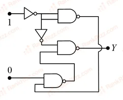
In the given circuit, value of Y is:
SOLUTION
Let the output of the top NAND gate be , the middle NAND gate be , and the bottom NAND gate be .
The output stage is a shared node tied directly to both upper outputs:
Output of the first NOT gate with input 1:
Since both inputs of the top NAND gate are tied to this node:
Output of the second NOT gate connected below it:
Evaluating the bottom NAND gate with one fixed input at 0:
Evaluating the middle NAND gate using its determined inputs:
Since the wire mesh forces a conflict where and attempt to drive the same node :
Tagged Logic gates and digital circuits. Machine-assigned, so read it as a strong shortlist rather than a verdict.