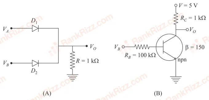
For Circuit (A): Analysis of the diode configuration
If VA=0 V and VB=0 V: Both D1 and D2 are reverse-biased (off) ⟹V0=0 V
If VA=5 V or VB=5 V: At least one diode conducts (on), pulling up the output node ⟹V0=5 V
This truth table (0,0→0; 0,1→1; 1,0→1; 1,1→1) corresponds exactly to an OR gate.
For Circuit (B): Analysis of the common-emitter BJT configuration
If VB=0 V: The base-emitter junction is cut off ⟹IC=0⟹V0=VCC−ICRC=5−0=5 V
If VB=5 V: Base current drives the transistor heavily into saturation ⟹V0=VCE(sat)≈0 V
This inversion logic (0→1 and 1→0) corresponds exactly to a NOT gate.