JEE MAIN 2022 · 25 JUL S1+4 / −1EASYTRANSCRIBED
JEE Main 2022 Physics question — Logic gates and digital circuits
In the circuit, the logical value of or when potential at or is and the logical value of or when potential at or is .
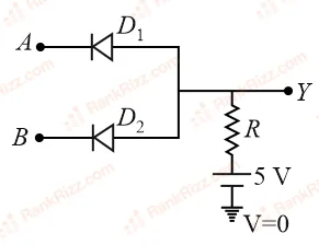
The truth table of the given circuit will be:
SOLUTION
We need to determine the correct truth table for the given diode logic circuit.
1. Analyze the Circuit Components and Logic Levels
From the schematic :
- The inputs and are connected to the cathodes (the pointy/bar side) of the ideal diodes and .
- The anodes (p-side) of both diodes are tied together to the output terminal .
- The output terminal is connected through a resistor to a supply voltage.
- Logical High (1):
- Logical Low (0): (Ground)
2. Evaluate the State Combinations
- Case 1: Both inputs are low ()
Both diodes have on their anode side (via resistor ) and on their cathode side. This makes both diodes forward-biased (conducting). They act as short circuits to ground, pulling the output voltage at down to .
- Case 2: One input is low and the other is high ( or )
The diode connected to the input becomes forward-biased and conducts, creating a direct path to ground. This forces the entire shared anode junction voltage down to . The other diode (connected to ) will be reverse-biased (non-conducting).
- Case 3: Both inputs are high ()
Both sides of the diodes are at a potential of . Because there is no potential difference across them to turn them on, no current flows through the diodes (they remain non-conducting). Since no current flows through the resistor , there is no voltage drop across it, leaving the output terminal at the supply potential of .
3. Establish the Truth Table
The circuit behaves exactly like a standard digital AND gate:
| 0 | 0 | 0 |
| 1 | 0 | 0 |
| 0 | 1 | 0 |
| 1 | 1 | 1 |
Conclusion
The truth table corresponds directly to Option A.
Tagged Logic gates and digital circuits. Machine-assigned, so read it as a strong shortlist rather than a verdict.