JEE MAIN 2025 · 02 APR S2+4 / −1EASYTRANSCRIBED
JEE Main 2025 Physics question — Logic gates and digital circuits
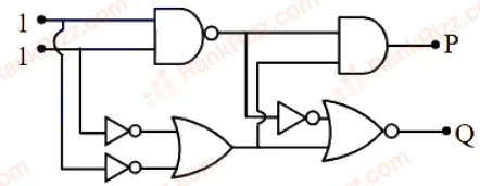
In the digital circuit shown in the figure, for the given inputs the P and Q values are :
SOLUTION
The top-left NAND gate receives inputs :
This feeds directly into the top AND gate. Since any input of to an AND gate forces a low output, is immediately determined:
The two left NOT gates receive inputs , turning them into .
The first OR gate processes these zeros:
This splits and travels to two places:
Directly to the bottom input of the final NOR gate .
Through the middle-right NOT gate (which inverts the first NAND's into a ) .
Finally, the NOR gate processes inputs :
Tagged Logic gates and digital circuits. Machine-assigned, so read it as a strong shortlist rather than a verdict.