Semiconductor Electronics
PHYSICS · 6 IDEAS · 252 PAST QUESTIONS · JEE MAIN + ADVANCED · 2004–2026
HOW TO USE THIS SHEET
One past question per idea, most-asked idea first; each is the most recent time the examiner set it. Answer it cold. Check your answer at the address printed beside it — there is no key in this sheet. An idea here is one syllabus topic — the finest tag our past questions carry. A topic can hold more than one technique, so treat each question as the door into an idea, not the whole of it.
- 01Logic gates and digital circuitsset 85×
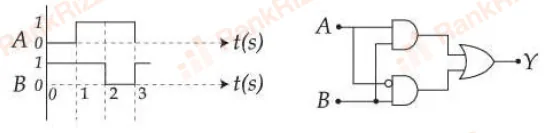
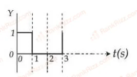
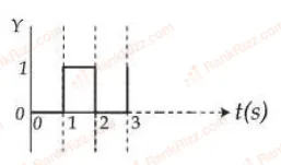
The output for the given inputs and to the circuit is :
- (A)
- (B)
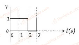
- (C)
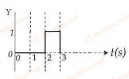
- (D)
CHECK IT: rankrizz.com/jee-main/physics/semiconductor-electronics/q/8-apr-2026-s2-q45
- (A)
- 02p-n junction diode and its characteristicsset 55×
In a semiconductor p-n diode, the doping concentrations on p-side has atoms/cm³ and the n-side has atoms/cm³respectively. Which one of the following statements is true?
- (A)
Widths of depletion region on either side of the interface are equal
- (B)
The depletion region widths is more on p-side compared to that in n-side
- (C)
The depletion region width is more on n-side compared to that the p-side
- (D)
No depletion region forms because of unequal doping concentrations on p and n-sides
CHECK IT: rankrizz.com/jee-main/physics/semiconductor-electronics/q/5-apr-2026-s2-q45
- (A)
- 03Zener diode, LED, photodiode and solar cellset 49×
The maximum rated power of the LED is 2 mW and it is used in the circuit with input voltage of 5 V as shown in the figure below. The current through resistance is 0.5 mA.
The minimum value of the resistance of , to ensure that the LED is not damaged is _______ k.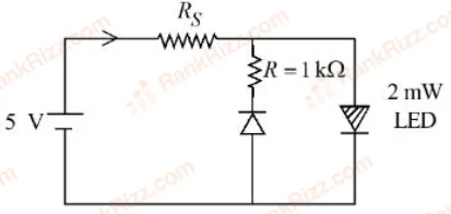
- (A)
6
- (B)
2
- (C)
4
- (D)
5
CHECK IT: rankrizz.com/jee-main/physics/semiconductor-electronics/q/6-apr-2026-s1-q39
- (A)
- 04Transistors (older syllabus)set 42×
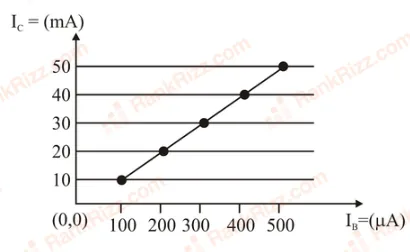
From the given transfer characteristic of a transistor in CE configuration, the value of power gain of this configuration is , for k, and k. The value of is _____.
Answer: ____________
CHECK IT: rankrizz.com/jee-main/physics/semiconductor-electronics/q/13-apr-2023-s1-q30
- 05Diode circuits and rectifiersset 12×
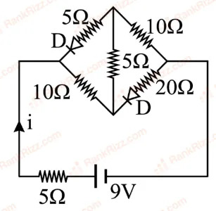
Find the value of current in the given circuit
- (A)
- (B)
- (C)
- (D)
Zero
CHECK IT: rankrizz.com/jee-main/physics/semiconductor-electronics/q/2026-physics-515699
- (A)
- 06Semiconductors: energy bands, intrinsic and extrinsicset 9×
This question has Statement 1 and Statement 2. Of the four choices given after the Statements, choose the one that best describes the two Statements. Statement 1: A pure semiconductor has negative temperature coefficient of resistance. Statement 2: On raising the temperature, more charge carriers are released into the conduction band.
- (A)
Statement 1 is false, Statement 2 is true.
- (B)
Statement 1 is true, Statement 2 is false.
- (C)
Statement 1 is true, Statement 2 is true, Statement 2 is not a correct explanation of Statement 1.
- (D)
Statement 1 is true, Statement 2 is true, Statement 2 is the correct explanation of Statement 1.
CHECK IT: rankrizz.com/jee-main/physics/semiconductor-electronics/q/2012-physics-499407
- (A)
Past questions are reproduced with their sitting. Not affiliated with NTA or the IITs. Every question on each idea: rankrizz.com/jee-main/physics/semiconductor-electronics